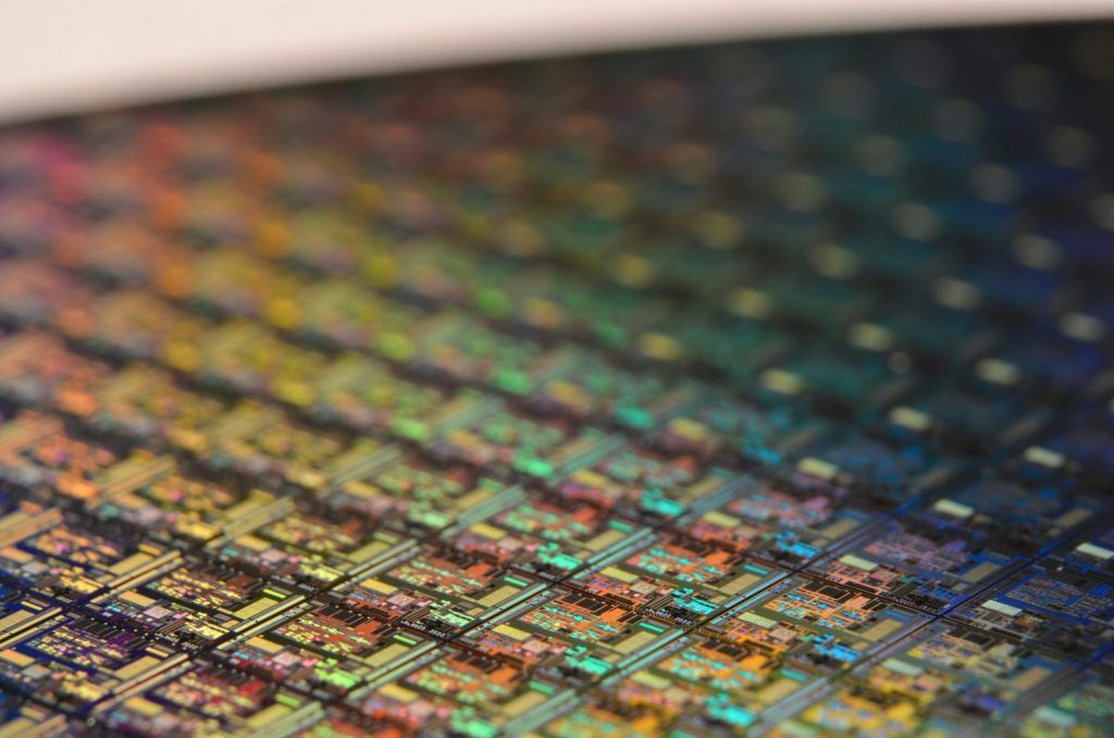
Thermal Atomic layer etching (ALE) is a recently developed technique to fabricate nanostructures with high precision. While not yet as scalable as other techniques, it shows promising application possibilities. To improve the power of integrated circuits such as CPUs, we need to build finer structures of transistors that can store the information used in electronic devices such as smartphones. Thermal ALE is a tool that can be used to address this challenge.
In order to create different structures, the semiconductor industry uses different bottom-up and top-down methods to deposit and remove materials at the nanoscale. Thermal ALE is one of the latter. By using this technique, researchers at MIT have built the smallest 3D transistor yet of only 2.5 nm across [i].
How does it work? [ii]
Thermal ALE was first reported in 2015 and can be viewed as the reverse of another important process known as atomic layer deposition (ALD). ALD was developed in 1977 and is used to add thin layers of compounds such as ZnS to a surface through controlled self-limiting steps [iii]. In ALE, the opposite happens where different materials can be etched away atomic layer by layer using mainly two processes.
For materials such as Al2O3, HfO2, and ZrO2, a fluorination process is firstly used. This first process depends on the material, and in other cases needs a conversion or oxidation step. It can be viewed as a way to prepare the surface for the second process which uses ligand exchange reactions to remove the material.
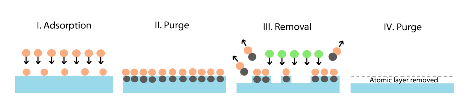
Figure 1: Schematic illustration of an ALE cycle. Step (I) shows the fluorination process, while step (III) shows the ligand exchange interactions to remove a layer from the surface. The purge steps (II&IV) are used to remove excess reagents or products.
On the one hand, the widely used etching technique, reactive ion etching (RIE) which uses plasma, is a lot quicker, requires lower temperatures, and has the desired properties of being selective and directional. On the other hand, the plasma does some damage to the surface and is not as reliable as thermal ALE.
A sort of in-between method developed in 1988 [iv], plasma ALE, has some of the same advantages as thermal ALE. Plasma ALE is a directional etch (only removing material in one direction), whereas thermal ALE is isotropic (etching in all directions at a time). Both etching types are needed and for certain 3d structures, the latter becomes especially important.
Outlook
As semiconductor devices become smaller, both thermal ALE and plasma ALE are becoming increasingly attractive methods to reach the demands of reliability and precision. Currently, they are expensive options, but this could be less of a concern with the increasing demand for more powerful electronic devices. Additionally, as a big research area, new ALE techniques are being developed for a range of materials that supports the wider use of the methods.
If you’d like to learn more about nanotechnology, please subscribe to our newsletter and stay tuned for upcoming posts.
References
[i] MIT News, Engineers produce smallest 3-D transistor yet, Dec 2018, accessed at https://news.mit.edu/2018/smallest-3-d-transistor-1207
[ii] Chang Fang et. al, Thermal atomic layer etching: Mechanism, materials and prospects, Dec 2018, accessed at https://www.sciencedirect.com/science/article/pii/S1002007118304623
[iii] Richard W. J. et al., A brief review of atomic layer deposition: from fundamentals to applications, June 2014, accessed at https://www.sciencedirect.com/science/article/pii/S1369702114001436
[iv] Keren J. K., et al., overview of atomic layer etching in the semiconductor industry, 2015, accessed at https://avs.scitation.org/doi/10.1116/1.4913379